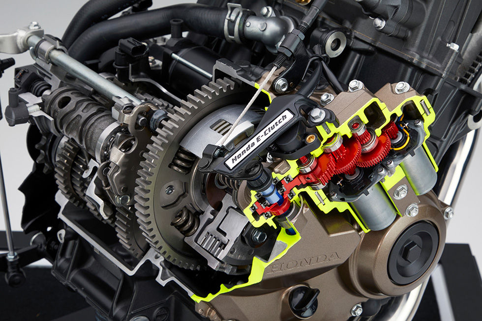
Honda Develops World’s First Honda E-Clutch for Motorcycles
Honda Motor Co., Ltd has developed the world’s first(1) Honda E-Clutch system for motorcycles that enables smooth starting and gear shifting without the need for the rider to operate the clutch lever(2), by automatically controlling the clutch of the multi-gear manual motorcycle transmission.
The Honda E-Clutch is electronic control technology that realizes natural and smooth riding through instantaneous, fine-tuned clutch control without the rider needing to operate the clutch lever, for optimum performance in situations where the driving force changes, such as starting, stopping, and shifting gears.To meet a wide range of rider demands, the clutch can be operated manually like a normal manual transmission motorcycle by gripping the clutch lever, even when the clutch is being controlled electronically.As Honda E-Clutch is a lightweight and compact system, it can be installed without major changes to existing engine layouts. Honda plans to apply Honda E-Clutch to its FUN motorcycle models over time.
Honda will continue to develop new technologies that improve the quality of the riding experience and provide motorcycles that meet the tastes of a wide range of riders who seek the joy of riding.
Honda E-Clutch
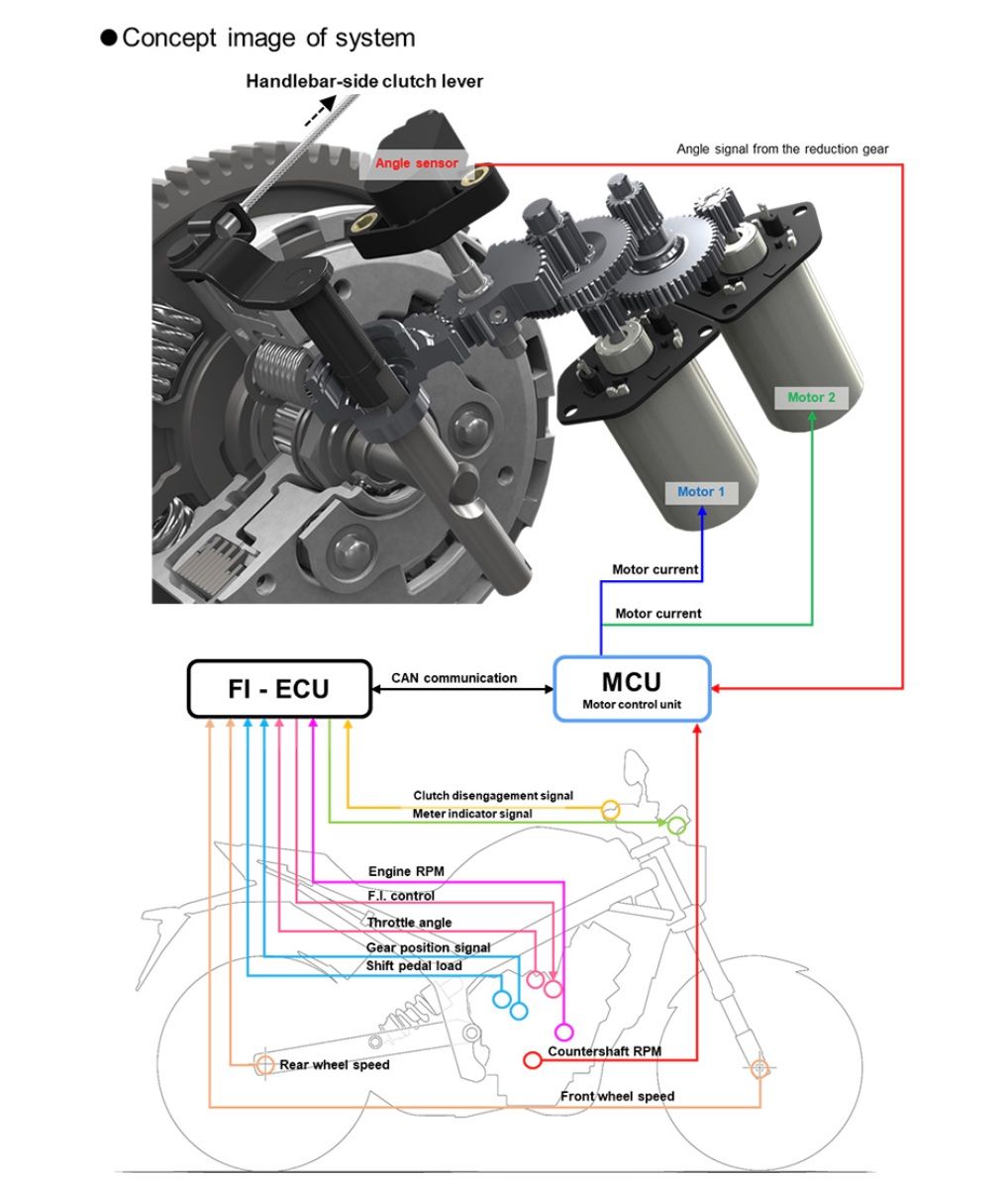
System Overview
The Honda E-Clutch electronically controls the power transmission mechanism similar to a conventional manual single clutch or manual transmission mechanism, combining engine-coordinated control (ignition timing, fuel injection, etc.) and clutch-coordinated control according to vehicle conditions (vehicle / engine speed, throttle position, gear position, shift pedal load detection, etc.), to respond to the rider’s inputs. In addition, manual clutch operation by using the clutch lever and the motorized clutch control are independent, enabling the rider to intervene manually, realizing both manual operation and clutch control by motor.The system can be turned on or off. When the system is on, clutch operation is controlled automatically by default, and the rider can temporarily switch to manual clutch operation by using the clutch lever. When the system is off, the rider must operate the clutch with the clutch lever at all times (starting, shifting gears, and stopping).
Overview image of Honda E-Clutch system
(1) according to Honda research (as of October 2023) (2) Gear shift pedal operation is required to change gears
TANAKA Develops First High-Entropy Alloy Powder Comprised Entirely of Precious Metals
With the establishment of five different precious metals alloy powder production methods
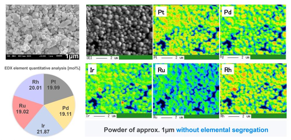
TOKYO, Oct 27, 2023 – (JCN Newswire) – TANAKA Kikinzoku Kogyo K.K., a core company of the TANAKA Precious Metals Group, has developed a high-entropy alloy powder composed entirely of precious metals with a fine particle size of 10um or less, high crystallinity and excellent composition uniformity. This is the world’s first high-entropy alloy powder composed entirely of five precious metals: platinum (Pt), palladium (Pd), iridium (Ir), ruthenium (Ru), and rhodium (Rh). TANAKA has established a mass production process and will provide samples in October.
TANAKA established the five precious metal alloy powders and their production methods used in this product, and obtained a basic patent in June 2023[1]. This product’s precious metal alloy powder comprises only five elements that maintain the corrosion resistance, electrical conductivity and other excellent properties of precious metals. They are micro-order[2] alloy powders that are easy to use in industrial applications.
Unlike conventional nano-order precious metal high-entropy alloys, the new alloy is stable due to its large crystallite size, and it satisfies the inherent requirements of alloys, such as improved mechanical strength, corrosion resistance, and controlled thermal expansion. The new alloy powder is expected to improve the functions and properties of precious metal alloys, whose properties vary greatly depending on the composition ratio of the alloy.
TANAKA develops the world’s first high-entropy alloy powder comprised of precious metals [Image: TANAKA Precious Metals]
The precious metal alloy of this product is in powder form, though it can also be utilized in paste form, which is often used in various circuits and sensors, in addition to modelling using a 3D printer and rod forming (forming rod-shaped material by solidifying powder). Furthermore, high-entropy alloys’ high strength and high heat resistance properties are expected to be utilized in catalysts and conductive films that require high durability, among other applications.
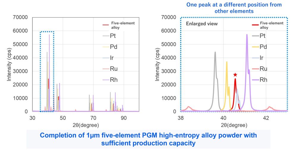
[1] Patent No. 7300565 related to high-entropy alloy powder was granted on June 29, 2023. The precious metal alloy powder in this product is defined as (1) precious metal alloy powder consisting of an alloy of five or more precious metal elements, (2) average particle size of 10µm or less, (3) crystallite size of 60nm or more, and (4) one peak observed in the range of diffraction angle 2θ of 38 to 44° in the X-ray diffraction spectrum.
[2] Order: A term used in physics, engineering, and other fields to roughly express the magnitude of a number. It represents the number of digits or degrees of a unit.
Component and surface analysis of high-entropy alloy powder
X-ray diffraction spectra of high-entropy alloy powder and various precious metal powders.
About High-Entropy Alloys
High-entropy alloys contain five or more elements in equal amounts and are characterized by the absence of major elements that make up most of the alloy. They have been attracting attention as a new category of metallic materials in recent years. Research and development on high-entropy alloys is being conducted worldwide, as the properties of the metals and precious metals contained in these alloys can simultaneously produce properties such as high strength, high heat resistance and the possibility of creating new properties.
About TANAKA Precious Metals
Since its foundation in 1885, TANAKA Precious Metals has built a portfolio of products to support a diversified range of business uses focused on precious metals. TANAKA is a leader in Japan regarding the volumes of precious metals handled. For many years, TANAKA has manufactured and sold precious metal products for industry and provided precious metals for jewellery and other assets. As precious metals specialists, Group companies in Japan and worldwide collaborate on manufacturing, sales, and technology development to offer a full range of products and services. With 5,355 employees, the group’s consolidated net sales for the year ending March 31, 2023, was 680 billion yen.
Global industrial business website https://tanaka-preciousmetals.com/en/
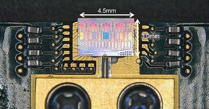
NEC develops 150 GHz Antenna-on-Chip transmitter IC chip for Beyond 5G/6G radio equipment
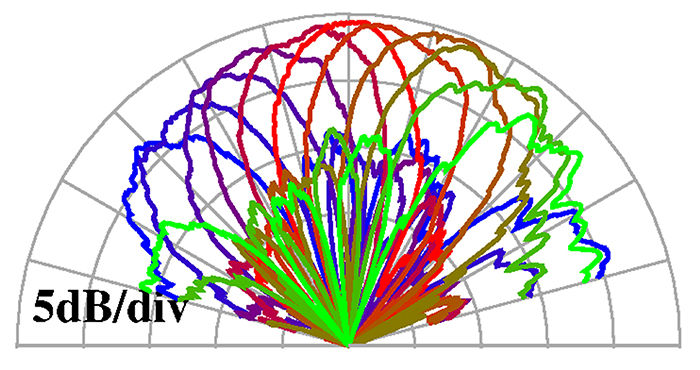
TOKYO, Oct 12, 2023 – (JCN Newswire) – NEC Corporation (TSE: 6701) has developed a 150 GHz transmitter IC chip and supporting technologies in preparation for Beyond 5G and 6G mobile access radio communication systems. According to an NEC survey, this is the first demonstration of preferred beam steering performance with 4-channel Antenna-on-Chip (AoC) IC technology using On the Air (OTA) radiation pattern measurement. Based on innovative RF circuit design technology, it has become possible to integrate 150 GHz phased array antenna elements, phase shifters and transmission amplifiers into a single chip. The 22-nm SOI-CMOS technology used for manufacturing this IC is cost effective, suitable for mass production, and has the ability to support large scale integration of digital, analog and RF functionalities in a chip. This allows for both higher frequencies and smaller sizes, which also contributes to lower Total Cost of Ownership (TCO) and potentially accelerates social implementation.
Development of a 150 GHz transmitter IC chip and supporting technologies
Beyond 5G and 6G are expected to provide 100 Gbps class broadband communications that are more than ten times faster than 5G. To achieve this, it is effective to utilize the sub-terahertz band (100GHz to 300GHz), which can secure a wide bandwidth of 10GHz or more. In particular, the D-band (130 GHz to 174.8 GHz), which is already assigned for fixed wireless communication systems worldwide, is expected to contribute to early social implementation. However, since the sub-terahertz band is subject to large propagation losses, large interconnection losses and device performance is near its limit, there is a need for the development of highly directional, high-gain antenna technology and its beam steering technology. To overcome these challenges, NEC developed a new IC chip that supports the 150GHz band. Going forward, NEC will continue to develop advanced technologies with the aim of contributing to the commercialization of 6G that is expected in the 2030s.
This research is supported by the Ministry of Internal Affairs and Communications in Japan (JPJ000254). NEC will present further details on this technology at the 2023 IEEE BiCMOS and Compound Semiconductor Integrated Circuits and Technology Symposium (BCICTS) in Monterey, CA, USA, October 15 to 18, 2023. NEC also presented the key principle and implementation of the “Switching Gain based Phase Shifter” at the European Microwave Integrated Circuits Conference 2023 held in Berlin, Germany, in September 2023.
About NEC CorporationNEC Corporation has established itself as a leader in the integration of IT and network technologies while promoting the brand statement of “Orchestrating a brighter world.” NEC enables businesses and communities to adapt to rapid changes taking place in both society and the market as it provides for the social values of safety, security, fairness and efficiency to promote a more sustainable world where everyone has the chance to reach their full potential. For more information, visit NEC at https://www.nec.com.
NEC Corporation (TSE: 6701) has succeeded in developing the world’s first high-sensitivity uncooled infrared image sensor that uses high-purity semiconducting carbon nanotubes (CNTs) in the infrared detection area. This was accomplished using NEC’s proprietary extraction technology. NEC will work toward the practical application of this image sensor in 2025.
Infrared image sensors convert infrared rays into electrical signals to acquire necessary information, and can detect infrared rays emitted from people and objects even in the dark. Therefore, infrared image sensors are utilized in various fields to provide a safe and secure social infrastructure, such as night vision to support automobiles driving in the darkness, aircraft navigation support systems and security cameras.
There are two types of infrared image sensors, the “cooled type,” which operates at extremely low temperatures, and the “uncooled type,” which operates near room temperature. The cooled type is highly sensitive and responsive, but requires a cooler, which is large, expensive, consumes a great deal of electricity, and requires regular maintenance. On the other hand, the uncooled type does not require a cooler, enabling it to be compact, inexpensive, and to consume low power, but it has the issues of inferior sensitivity and resolution compared to the cooled type.
In 1991, NEC discovered CNTs for the first time in the world and is now a leader in research and development related to nanotechnology. In 2018, NEC developed a proprietary technology to extract only semiconducting-type CNTs at high purity from single-walled CNTs that have a mixture of metallic and semiconducting types. NEC then discovered that thin films of semiconducting-type CNTs extracted with this technology have a large temperature coefficient of resistance (TCR) near room temperature.
The newly developed infrared image sensor is the result of these achievements and know-how. NEC applied semiconductor-type CNTs based on its proprietary technology that features a high TCR, which is an important index for high sensitivity. As a result, the new sensor achieves more than three times higher sensitivity than mainstream uncooled infrared image sensors using vanadium oxide or amorphous silicon.
The new device structure was achieved by combining the thermal separation structure used in uncooled infrared image sensors, the Micro Electro Mechanical Systems (MEMS) device technology used to realize this structure, and the CNT printing and manufacturing technology cultivated over many years for printed transistors, etc. As a result, NEC has succeeded in operating a high-definition uncooled infrared image sensor of 640 x 480 pixels by arraying the components of the structure.
Part of this work was done in collaboration with Japan’s National Institute of Advanced Industrial Science and Technology (AIST). In addition, a part of this achievement was supported by JPJ004596, a security technology research promotion program conducted by Japan’s Acquisition, Technology & Logistics Agency (ATLA).
Going forward, NEC will continue its research and development to further advance infrared image sensor technologies and to realize products and services that can contribute to various fields and areas of society.
About NEC Corporation
NEC Corporation has established itself as a leader in the integration of IT and network technologies while promoting the brand statement of “Orchestrating a brighter world.” NEC enables businesses and communities to adapt to rapid changes taking place in both society and the market as it provides for the social values of safety, security, fairness and efficiency to promote a more sustainable world where everyone has the chance to reach their full potential. For more information, visit NEC at www.nec.com.
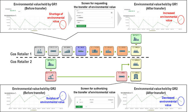
Three partners build a demonstration system for CO2NNEX for e-methane, a digital platform for visualizing CO2 emissions across e-methane value chain and transferring e-methane’s environmental value Feb 15, 2023 11:17 JST
Three partners build a demonstration system for CO2NNEX for e-methane, a digital platform for visualizing CO2 emissions across e-methane value chain and transferring e-methane’s environmental value Feb 15, 2023 11:17 JST
Three partners build a demonstration system for CO2NNEX for e-methane, a digital platform for visualizing CO2 emissions across e-methane value chain and transferring e-methane’s environmental value Feb 15, 2023 11:17 JST
MHIEC Builds a New Waste-to-Energy Plant with 194 Tons Per Day-Capacity in Konan City, Aichi Prefecture, Japan Feb 14, 2023 09:27 JST
NEC successfully demonstrated Multi-Vendor Near-RT RIC Integration in O-RAN Global PlugFest 2022 Feb 13, 2023 15:11 JST
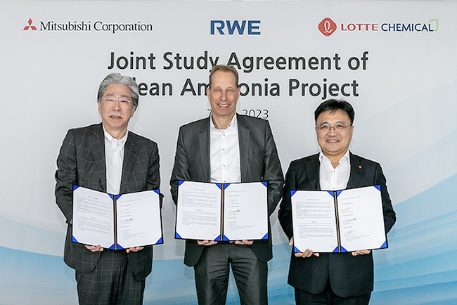
RWE, LOTTE CHEMICAL Corporation and Mitsubishi Corporation enter into a Joint Study Agreement to develop a clean ammonia project in Port of Corpus Christi in Texas, USA Feb 08, 2023 16:37 JST
inter airport Southeast Asia 2023 returns in March; exhibition completely sold out after four-year hiatus Feb 16, 2023 17:35 JST
富士通、トルコ・シリア大地震による被害への支援について Feb 16, 2023 16:30 JST
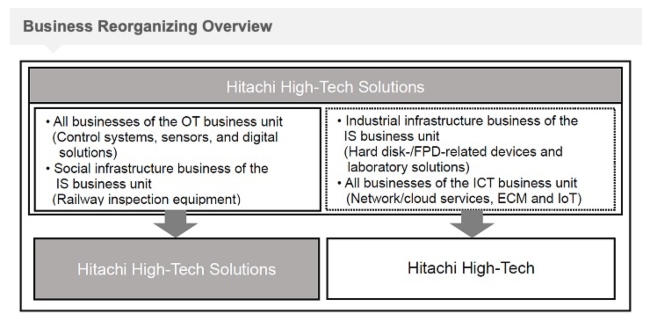
日立ハイテク、社会インフラの課題解決力強化に向けて、日立ハイテクソリューションズを再編 Feb 16, 2023 15:30 JST
NEC launches Value Added xHaul Solution Suite with Open Ecosystem Feb 16, 2023 16:15 JST
Reorganizing Hitachi High-Tech Solutions to Strengthen Capabilities for Solving Social Infrastructure Issues Feb 16, 2023 14:31 JST
三菱電機、ビル用マルチエアコン室内ユニット「天井カセット形4方向吹出し」新製品発売 Feb 16, 2023 13:30 JST
三菱重工、グループ表彰制度「Best Innovation」で地球環境負荷低減に貢献する活動を表彰 Feb 16, 2023 12:30 JST
サステナブルな旅という視点からみた CNN「The Journey Matters」の東京探検 Feb 16, 2023 11:00 JST
サステナブルな旅という視点からみた CNN「The Journey Matters」の東京探検 Feb 16, 2023 11:00 JST
MHI Group Presents “Best Innovation 2022” Awards for Activities that Contribute to Mitigating Impacts on the Global Environment Feb 16, 2023 10:35 JST


")


