
TANAKA Establishes Transfer Technology for its Sintered Gold (Au) Bonding Technology, AuRoFUSE(TM) Preforms
The smooth application on substrates with intricate shapes will enhance semiconductor efficiency through boosted miniaturization of semiconductor circuitry and higher combination for different kinds of chips
TOKYO, Mar 3, 2026 – (JCN Newswire) –TANAKA PRECIOUS METAL TECHNOLOGIES Co., Ltd. (Head workplace: Chuo-ku, Tokyo; Representative Director & & CEO: Koichiro Tanaka), a business participated in the commercial rare-earth elements company of TANAKA, today revealed a gold bump* 1 transfer innovation for the sintered gold (Au) bonding innovation, AuRoFUSE ™ PreformsThis innovation permits AuRoFUSE ™ Preforms (gold bumps) to be formed even on semiconductor chips and substrates* 2 with intricate structures.
Benefits of having the ability to move gold bumps
In this innovation, initially, gold bumps are formed on a substrate(transfer substrate). The gold bumps are moved to the target semiconductor chip or substrate. Openings are developed on the silicon substrate utilized as the transfer substrate, and gold bumps are formed in them. By filling the whole opening, the gold bump is held by the substrate, getting rid of the danger of dropping throughout the procedure. Throughout transfer, the gold bump diminishes under heat-treatment, forming a small space in between the opening and the gold bump. This permits simple extraction of gold bumps by the application of a force in the vertical instructions. 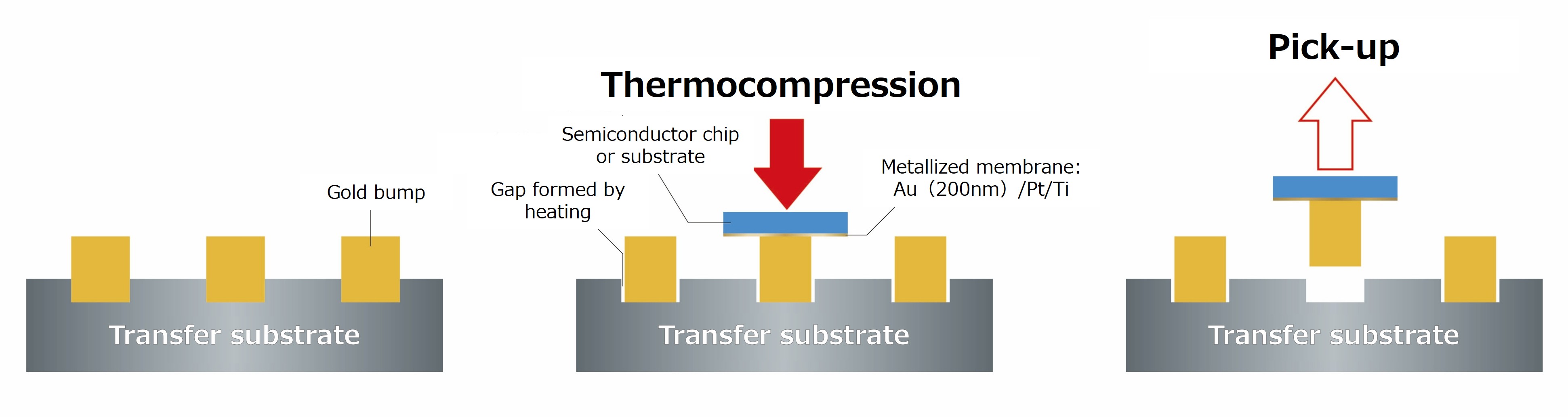
As the conventional gold bump development procedure is a technique that straight forms bumps on the target semiconductor chip or substrate, it is tough to deal with target chips and substrates with complicated shapes, such as protrusions, damages, or open holes due to concerns such as irregular withstand heights.
In this present transfer innovation, gold bumps are made independently and can be moved just to the target places. This enables the innovation to likewise be used to complicated shapes. It can likewise be utilized with semiconductor chips and substrates that are hard to procedure utilizing photolithography* 3 due to issues about damage from removing options and others.
Production of transfer substrate and transfer and bonding procedure
(1) Preparation of silicon substrate as transfer substrate
(2)Application of photoresist to silicon substrate
(3)Exposure and advancement of target pattern
(4) Etching of silicon substrate to produce holes
(5) Application of AuRoFUSE ™ utilizing a squeegee, and so on.
(6)Vacuum drying of AuRoFUSE ™ at space temperature level and removing excess gold particles on the withstand
(7)Removal of withstand to total transfer substrate
(8)Placement of transfer substrate on target (semiconductor chip or substrate )for gold bump development, thermocompression at 10 MPa and 150 ℃ for one minute, followed by vertical lifting of substrate to move gold bumps
(9) Bonding of post-transfer target through thermocompression at 20 MPa and 200 ℃ for 10 seconds
An illustration of the conventional gold bump development procedure is offered in the “Manufacturing of AuRoFUSE ™ Preforms” area for referral on TANAKA’s site.
About the sintered gold bonding innovation “AuRoFUSE ™ Preforms”
Established by TANAKA, “AuRoFUSE ™ Preforms” is a bonding innovation that forms bumps of all sort of shapes utilizing a paste consisting of gold particles and a natural solvent. Through a thermocompression bonding procedure (20 MPa at 200 ℃ for 10 seconds), AuRoFUSE ™ Preforms displays compression of around 10% in the compressive instructions while revealing very little contortion in the horizontal instructions. This provides adequate bonding strength* 4 for useful applications. With the primary part being gold, which has a high level of chemical stability, AuRoFUSE ™ Preforms likewise offers exceptional dependability after installing.
This innovation allows miniaturization of semiconductor circuitry and higher combination (greater density) for numerous kinds of chips. It is anticipated to add to the requirements for miniaturization and much better efficiency of semiconductors, which have actually been increasing over the last few years, consisting of optical gadgets such as light-emitting diodes (LEDs) and semiconductor lasers (LDs), usage in digital gadgets such as desktop computers, smart devices, in addition to in-vehicle parts, micro-electromechanical systems (MEMS), and such.
Typically, the primary approaches utilized in bump development innovation are soldering and plating. As solder tends to spread out outside in molten state, there was the danger of short-circuiting through contact in between electrodes as the bump pitch ends up being finer. Plating can attain a great pitch, however since relatively greater pressures are needed throughout bonding, there is the possibility of triggering chip damage. For recommendation, an illustration detailing the benefits of this innovation compared to soldering and plating products is supplied in the “Comparison of AuRoFUSE ™ Preforms with Other Materials” area on TANAKA’s site. This innovation was established to deal with these concerns for usage in next-generation high-density installing and photonics-electronics combination gadgets.
AuRoFUSE ™ and TANAKA’s gold products
AuRoFUSE ™ is a paste-type bonding product including a mix of gold particles, with the particle size managed to be submicron sized, and a natural solvent. Compared to the melting point of gold (roughly 1,064 ℃), bonding is possible at a low temperature level of around 200 ℃.
Gold is a product with low electrical resistance and very high thermal conductivity. In power semiconductors that deal with big currents and high-density chips that dissipate a lot of heat, it can effectively dissipate heat and limitation energy loss. Amongst rare-earth elements, it is likewise especially resistant to oxidation and has steady homes, making it less prone to rust after installing and ion migration (a phenomenon in which metals move and trigger brief circuits). This permits it to preserve high dependability over extended periods of time.
TANAKA is extremely experienced in rare-earth element product advancement innovations, established given that its facility. It has actually utilized these innovations to carry out advancement of rare-earth element products, such as gold, which plays an essential function in the semiconductor field. With a system that incorporates the whole chain of procedures, from basic material procurement to product advancement, production, and recycling, TANAKA will add to the advancement of semiconductor innovations and the awareness of a sustainable society while efficiently utilizing minimal rare-earth element resources.
* 1 Bumps: Protruding electrodes
* 2 Substrate: Board that electrically and mechanically supports semiconductor chips installed on it
* 3 Photolithography: Technology for forming great circuit patterns on substrates
* 4 Bonding: Refers to shear strength (strength identified through application of a lateral load throughout screening)
About TANAKA
Considering that its structure in 1885, TANAKA has actually developed a portfolio of items to support a varied variety of company utilizes concentrated on rare-earth elements. TANAKA is a leader in Japan concerning the volume of rare-earth elements it manages. Over several years, TANAKA has actually made and offered rare-earth element items for market and supplied rare-earth elements in such kinds as precious jewelry and possessions. As rare-earth elements professionals, all Group business in Japan and around the world team up on production, sales, and innovation advancement to use a complete variety of product or services. With 5,591 workers, the group’s combined net sales for the ended December 2024 were 846.9 billion yen.
TANAKA Industrial Precious Metal Materials Portal
https://tanaka-preciousmetals.com
Item questions
TANAKA PRECIOUS METAL TECHNOLOGIES Co., Ltd.
https://tanaka-preciousmetals.com/en/inquiries-on-industrial-products/
Press questions
TANAKA PRECIOUS METAL GROUP Co., Ltd.
https://tanaka-preciousmetals.com/en/inquiries-for-media/
News release: https://www.acnnewswire.com/docs/files/20260303_EN.pdf